- 您现在的位置:买卖IC网 > Sheet目录368 > W631GG6KB-15 (Winbond Electronics)IC DDR3 SDRAM 1GBIT 96WBGA
�� �
�
�W631GG6KB�
�T0�
�T1�
�T2�
�T3�
�T4�
�T5�
�T6�
�T7�
�T8�
�T9�
�T10�
�CK#�
�CK�
�Command� *3�
�WRITE�
�NOP�
�NOP�
�NOP�
�NOP�
�NOP�
�NOP�
�NOP�
�NOP�
�NOP�
�NOP�
�WL� =� AL� +� CWL�
�Address� *4�
�Bank�
�Col� n�
�t� DQSS� (min)�
�t� WPRE(min)�
�t� DQSS� t� DSH�
�t� DSH�
�t� DSH�
�t� DSH�
�t� WPST(min)�
�DQS,� DQS#�
�t� DQSH(min)�
�t� DQSL�
�t� DQSH�
�t� DQSL�
�t� DQSH�
�t� DQSL�
�t� DQSH�
�t� DQSL�
�t� DQSH�
�t� DQSL(min)�
�t� DSS�
�t� DSS�
�t� DSS�
�t� DSS�
�t� DSS�
�DQ� *2�
�Din�
�n�
�Din�
�n+2�
�Din�
�n+3�
�Din�
�n+4�
�Din�
�n+6�
�Din�
�n+7�
�DM�
�t� DQSS� (nominal)�
�t� WPRE(min)�
�t� DSH�
�t� DSH�
�t� DSH�
�t� DSH�
�t� WPST(min)�
�DQS,� DQS#�
�t� DQSH(min)�
�t� DQSL�
�t� DQSH�
�t� DQSL�
�t� DQSH�
�t� DQSL�
�t� DQSH�
�t� DQSL�
�t� DQSH�
�t� DQSL(min)�
�t� DSS�
�t� DSS�
�t� DSS�
�t� DSS�
�t� DSS�
�DQ� *2�
�Din�
�n�
�Din�
�n+2�
�Din�
�n+3�
�Din�
�n+4�
�Din�
�n+6�
�Din�
�n+7�
�DM�
�t� DQSS�
�t� DQSS� (max)�
�t� WPRE(min)�
�t� DSH�
�t� DSH�
�t� DSH�
�t� DSH�
�t� WPST(min)�
�DQS,� DQS#�
�t� DQSH(min)�
�t� DQSL�
�t� DQSH�
�t� DQSL�
�t� DQSH�
�t� DQSL�
�t� DQSH�
�t� DQSL�
�t� DQSH�
�t� DQSL(min)�
�t� DSS�
�t� DSS�
�t� DSS�
�t� DSS�
�t� DSS�
�DQ�
�Din�
�n�
�Din�
�n+2�
�Din�
�n+3�
�Din�
�n+4�
�Din�
�n+6�
�Din�
�n+7�
�DM�
�TRANSITIONING� DATA�
�DON'T� CARE�
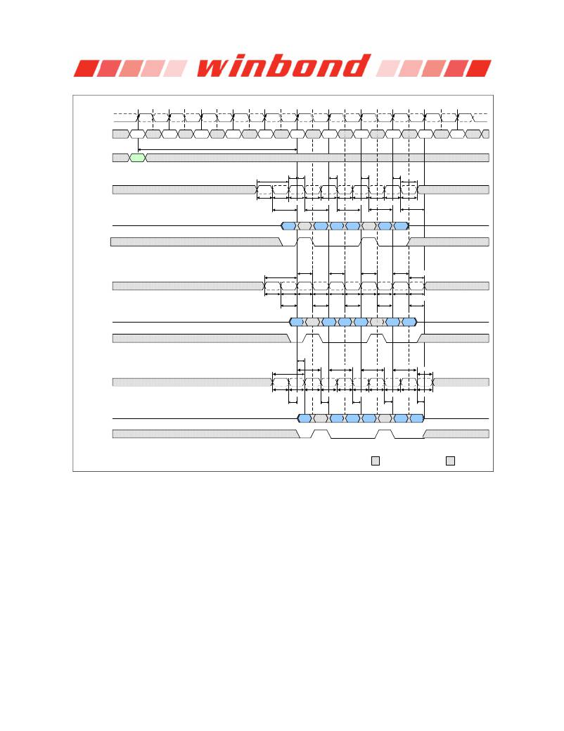
�Notes:�
�1.� BL8,� WL� =� 5� (AL� =� 0,� CWL� =� 5)�
�2.� Din� n� =� data-in� from� column� n.�
�3.� NOP� commands� are� shown� for� ease� of� illustration;� other� commands� may� be� valid� at� these� times.�
�4.� BL8� setting� activated� by� either� MR0� A[1:0]� =� 00� or� MR0� A[1:0]� =� 01� and� A12� =� 1� during� WRITE� command� at� T0.�
�5.� t� DQSS� must� be� met� at� each� rising� clock� edge.�
�Figure� 40� –� Write� Timing� Definition� and� Parameters�
�8.14.3� Write� Data� Mask�
�One� write� data� mask� (DM)� pin� for� each� 8� data� bits� (DQ)� will� be� supported� on� DDR3� SDRAMs,�
�consistent� with� the� implementation� on� DDR2� SDRAMs.� It� has� identical� timings� on� write� operations� as�
�the� data� bits� as� shown� in� Figure� 40,� and� though� used� in� a� unidirectional� manner,� is� internally� loaded�
�identically� to� data� bits� to� ensure� matched� system� timing.� DM� is� not� used� during� read� cycles.�
�Publication� Release� Date:� Dec.� 09,� 2013�
�Revision� A05�
�-� 57� -�
�发布紧急采购,3分钟左右您将得到回复。
相关PDF资料
W9412G6IH-5
IC DDR-400 SDRAM 128MB 66TSSOPII
W9412G6JH-5I
IC DDR SDRAM 128MBIT 66TSOPII
W9425G6EH-5
IC DDR-400 SDRAM 256MB 66TSSOPII
W9425G6JH-5I
IC DDR SDRAM 256MBIT 66TSOPII
W947D2HBJX5E
IC LPDDR SDRAM 128MBIT 90VFBGA
W948D2FBJX5E
IC LPDDR SDRAM 256MBIT 90VFBGA
W949D2CBJX5E
IC LPDDR SDRAM 512MBIT 90VFBGA
W971GG6JB25I
IC DDR2 SDRAM 1GBIT 84WBGA
相关代理商/技术参数
W631GG8KB-11
制造商:Winbond Electronics Corp 功能描述:IC DDR3 SDRAM 1GBIT 制造商:Winbond Electronics Corp 功能描述:IC DDR3 SDRAM 1GBIT 78WBGA
W631GG8KB-12
制造商:Winbond Electronics Corp 功能描述:DRAM Chip DDR3 SDRAM 1G-Bit 128Mx8 1.5V 制造商:Winbond Electronics Corp 功能描述:IC DDR3 SDRAM 1GBIT 制造商:Winbond Electronics Corp 功能描述:IC DDR3 SDRAM 1GBIT 78WBGA
W631GG8KB-15
制造商:Winbond Electronics Corp 功能描述:IC DDR3 SDRAM 1GBIT 制造商:Winbond Electronics Corp 功能描述:IC DDR3 SDRAM 1GBIT 78WBGA
W632
制造商:LUMINIS 制造商全称:LUMINIS 功能描述:Wall mount
W632GG6KB-11
制造商:Winbond Electronics Corp 功能描述:IC DDR3 SDRAM 2GBIT 96WBGA
W632GG8KB-11
制造商:Winbond Electronics Corp 功能描述:IC DDR3 SDRAM 2GBIT 78WBGA
W634
制造商:LUMINIS 制造商全称:LUMINIS 功能描述:Wall mount
W638
制造商:LUMINIS 制造商全称:LUMINIS 功能描述:Wall mount